BACKGROUND
A computer is useful because it is a device that can not only execute instructions but can also store and retrieve information along the way to aid in the execution of such instructions. Like everything else in an electronic computer, the component that handles this functionality (the memory subsystem) is made up of electronic circuits. In this article, I will like to share a high-level overview of what this circuitry looks like and how it operates. Electronic circuits are built from basic elements called logic gates (AND, OR, NAND, etc). It is advisable that the reader know these basic elements and understands how they operate as this will make it easier to follow along with the material. This Wikipedia article is a start.
Speaking of logic circuits, they can be classified under two broad type: Combinational and Sequential. Combinational circuits such as multiplexers or decoders compute outputs that depend solely on the combination of input they receive. Moreover, the chips that perform these operations cannot maintain state. That is, they simply spit out whatever output they produced based on the inputs they are provided. Sequential circuits, on the other hand, are able to ‘store’ the output of a prior computation and possibly use it as part of the input in subsequent operations.
The remainder of this article will discuss sequential circuits called the R-S Latch and Gated D-Latch and how they are used to build memory.
R-S LATCH
The R-S Latch is a simple sequential circuit that is capable of storing 1-bit of information. There are several ways to implement an R-S latch, but one of the simplest is shown in the image below.
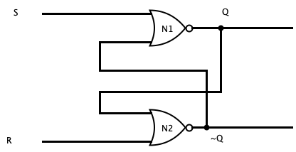
It consists of two NOR gates wired such that the output of one NOR gate is connected to the input of the other. In addition, the circuit has two inputs labeled S (set) and R (reset). It also has two outputs Q and ~Q. To understand how such a circuit works, we need to look at all the possible states the input can be in and their corresponding outputs.
CASE I: R=1, S=0
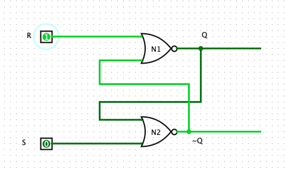
At some clock cycle T, if we assert the reset line, R and cleared the set (S) line, the output is Q=0 and ~Q=1. If at some time T+1, if we clear R and set S, then we get Q=1 and ~Q=0. Then we say out circuit stores value 1.
CASE II: R=0, S=1
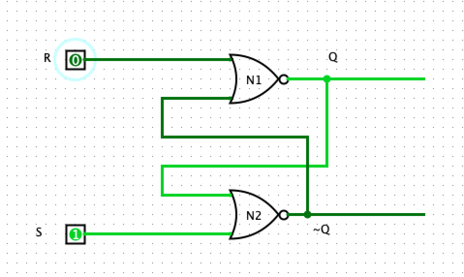 At some clock cycle T, if we assert the set (S) line and cleared the reset (R) line, our output is Q=1 and ~Q=0. If at some time T+1, if we clear S and set R, we get Q=0 and ~Q=1. We see that resetting the circuit means we now store the value 0.
CASE II: R=0, S=0
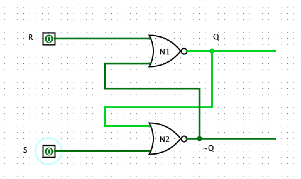 If both R and S are 0, then it means the value of our output Q is whatever the value was in the previous computation. If Q=1, setting or clearing S does not change the value store. However, setting R will flip Q to 0. Likewise, if Q=0, setting S=1 will make Q=1 and ~Q=0. While setting or resetting R will not change the value of Q.
CASE IV: R=1, S=1
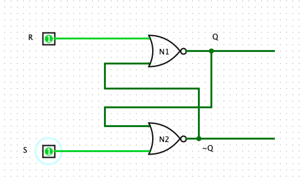 Asserting both the set and reset lines produces Q=0 and ~Q=0. One must make sure that both R and S are not asserted at the same time because the circuit does not behave deterministically in this state.
Putting all this together, we say that at some clock cycle T, the circuit produces some value Q which is 0 or 1 and represents the current state of the circuit. When R=0 and S=0, the circuit will ‘remember’ this value. Setting or clearing R and/or S will change the value currently stored in the circuit.
D LATCH
The R-S Latch has some shortcomings. We cannot control what data the circuit should hold and when the current data should be changed. This situation can be rectified using the D-Latch. The D-Latch uses the R-S Latch in addition to some additional gates to provide a data line for the data to be stored (D) and a write-enabled (WE) line to tell the circuit whether or not to update the value of the circuit. The result is shown on the circuit below.
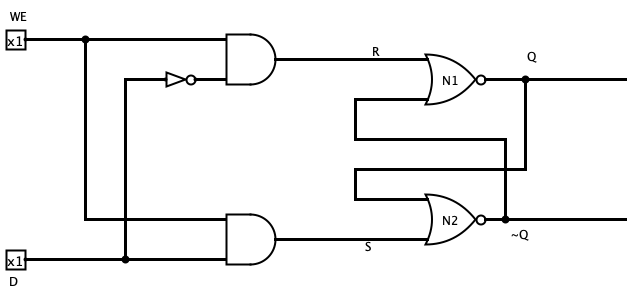
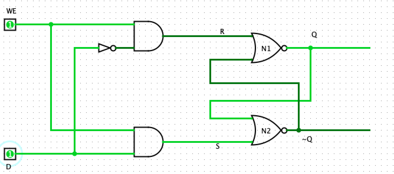
If we assert the WE line and the D line, then we see that the output Q has a value of 1. If D is not asserted, then Q=0 and the circuit will store 0.
Clearing the WE line will ensure that the value currently stored in the circuit is not modified.
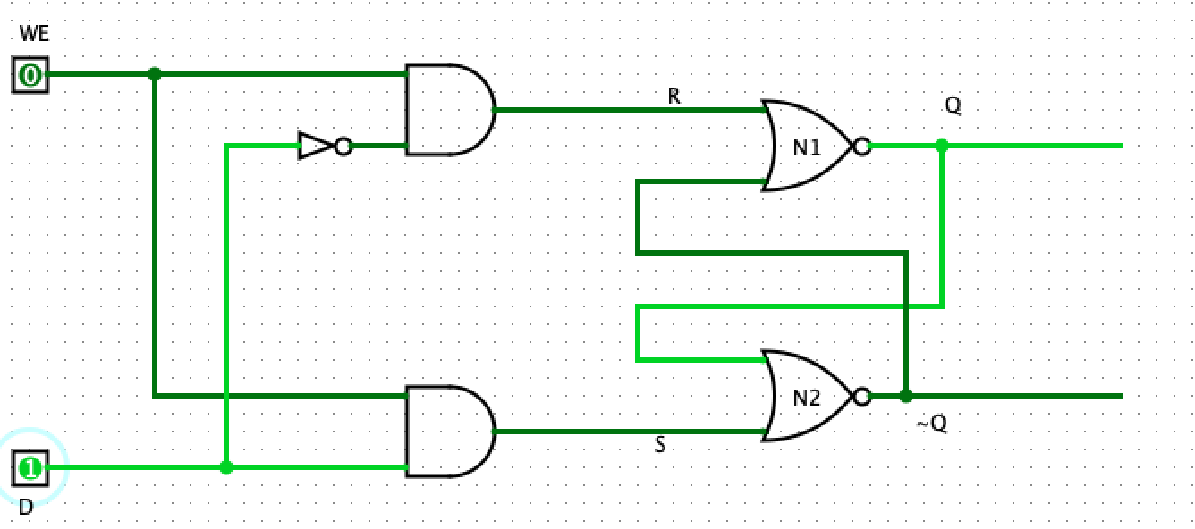
So far, we have a circuit that is able to store 1 bit of information. We provide the data on the D line and use the WE line to indicate whether the new data should be stored. Definitely, a circuit that stores 1 bit will not be very useful to a computer as most computers operate on multiples of 8-bit data.
REGISTERS
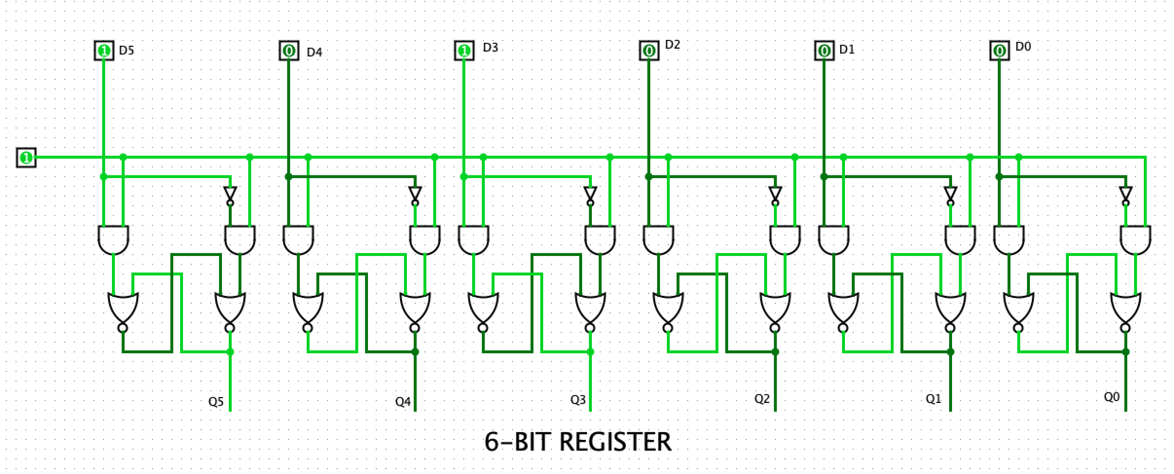
We can combine n D-Latch circuits to create an n-bit register. An array of 8 D Latches will give us an 8-bit register, 16 latches give a 16-bit register and so on. From the diagram below, we have a 5-bit register with the data fields set to 10100 with the WE line asserted. We, therefore, see that the output field also has 10100. We can go on to stack several of such registers to create larger banks of memory.
CONCLUSION
In this article, we followed the foundations of the memory subsystem. We started out with learning how to store 1 bit before creating an array of such circuits to store bigger numbers.